Advanced chip packaging FabLab project launched in Da Nang
The nearly $69-million project will be constructed on a 2,288-sq.m plot, with a total usable floor area of over 5,700 sq.m, divided into two main zones.
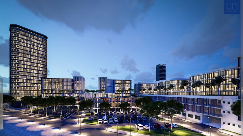
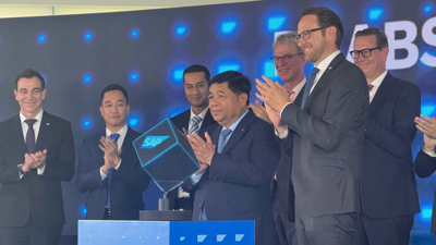
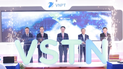
The Ministry of Science and Technology, in collaboration with the People's Committee of Da Nang city, held a launching ceremony on July 28 for the Advanced Packaging Technology Manufacturing Laboratory (Fab-Lab) project at the Da Nang Software Park No. 2 in the central city.
With a total investment of VND1.8 trillion ($68,8 million), the Fab-Lab project is a pioneering model in Vietnam’s semiconductor packaging sector.
It holds strategic significance for developing core technologies, directly implementing Politburo Resolution 57 (dated December 22, 2024) on breakthroughs in science and technology development, innovation, and digital transformation, as well as the National Semiconductor Industry Development Strategy to 2030, with a vision to 2050.
The project will be constructed on a 2,288-sq.m plot, with a total usable floor area of over 5,700 sq.m, divided into two main zones.
The first is a Lab zone dedicated to the research and development of advanced packaging technologies such as Fan-out Wafer Level Packaging (FOWLP), 2.5D/3D ICs, Silicon Interposers, and Silicon-Bridge technology.
The second is a Fab zone for pilot production on real wafers, equipped with modern machinery including lithography and wafer bonding systems, along with internationally standardized measurement and testing systems.
The project is scheduled for completion and is expected to become operational in the fourth quarter of 2026. It will have a designed capacity of 10 million units per year, serving both domestic and international markets.


